In this tutorial you will use an Intel® SoC FPGA to see how Field Programmable Gate Arrays (FPGAs) can be used to accelerate a complex mathematical function, boosting system performance and off-loading the CPU from a computationally intensive algorithm.
This design uses a Cyclone® V SoC FPGA to demonstrate a mathematical function that creates fractal images, known as the "Mandelbrot Set". The algorithm runs on the dual-core Arm Cortex*-A9 processor, and on a hardware accelerator inside the FPGA letting you see the difference in performance, and CPU load. As part of the tutorial, you will experiment with various hardware and software optimizations to see how they affect system performance.
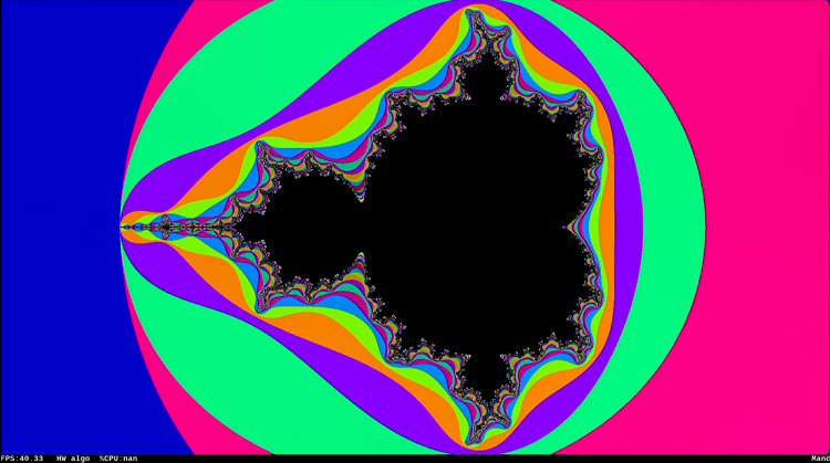
Figure 1. Fractal Image Display
- What is the Mandelbrot set and how is it computed?
-
This example is based on the Mandelbrot fractal, which is computed in the complex number plane. The Mandelbrot algorithm can be used to draw a color picture representing the points within the set as black, while those lying outside the set are assigned a color based on the number of iterations passed through the algorithm before they fall out of the set.
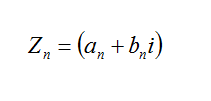
The algorithm is simply a continuous iteration of the following equation, where Z and C represent complex numbers. The initial value of Z0 is 0, and C represents the point on the complex plain that is being analyzed.
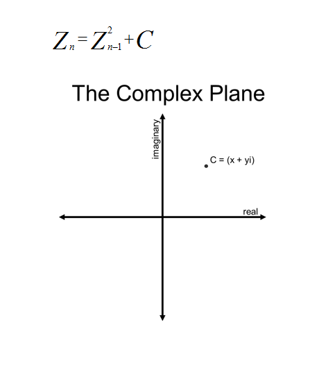
Figure 2. The Complex PlaneThe iteration of the Mandelbrot equation goes like this:
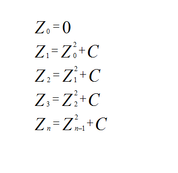
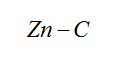
The iteration continues until either the maximum iteration count is met, or when the distance of Zn is at or greater than 2 from the value of C on the complex plane. A distance greater than 2 indicates points outside the Mandelbrot set.
Want to see the math? Read on . . .
The Mandelbrot equation can be minimized as follows, if we assume the complex numbers Z and C can be represented as follows:
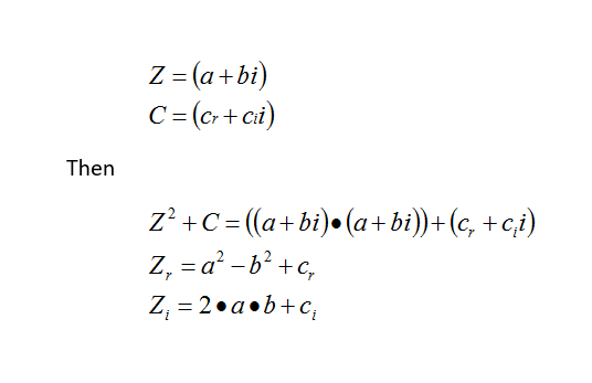
Once we have the new Zn, we need to calculate its distance from C.
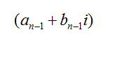
If the current Zn is:
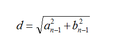
The distance is:
Which is equal to the previous Zn-1:
So, the distance is simply:
Or a distance greater than 2 would be:

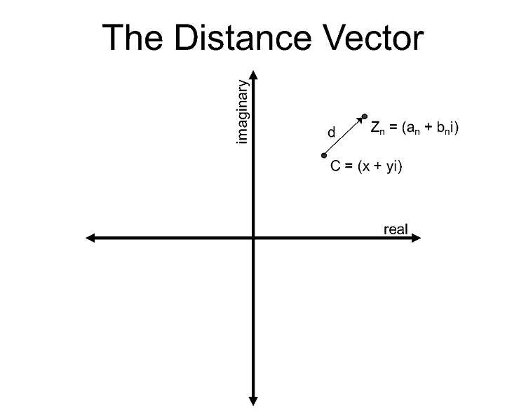
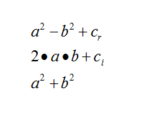
Figure 3. The Distance VectorThese minimizations of the Mandelbrot and distance computations result in three equations required to compute each iteration:
Here is an example of C code that performs this function. You can access the source code used by the processor in the Code Samples section.
int float_mandelbrot(float cr, float ci, int max_iter)
{
	float xsqr=0.0, ysqr=0.0, x=0.0, y=0.0;
	int iter=0;
	while( ((xsqr + ysqr) < 4.0) && (iter < max_iter) )
	{
		xsqr = x * x;
		ysqr = y * y;
		y = (2 * x * y) + ci;
		x = xsqr - ysqr + cr;
		iter++;
	}
	return(iter);
Level: beginner
Materials
Hardware
- HDMI monitor and cable
- Terasic DE10-Nano Development Kit
- MicroSD Card with Mandelbrot design loaded
To check the version of your Terasic DE10-Nano microSD Card, do the following:
- How do I know if my microSD Card contains the Mandelbrot design?
-
To check the version of your Terasic DE10-Nano microSD Card, do the following:
1. Use the micro-b USB cable to connect the board (USB OTG port) and your host system (Type-A end of the cable connects into a standard USB port on your computer).
2. If you've unplugged the power cable, plug it back into the board. Wait for the board to boot.
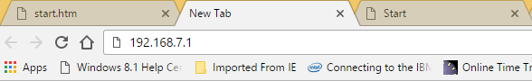
3. Open a web browser on your PC (Google Chrome* or Firefox* recommended), and type the IP address 192.168.7.1 into the URL pane.
4. You've now arrived at the webpage hosted by the Terasic DE10-Nano board. Navigate to the Resources tab, select Design Files, and click Get the Version of This SD Card button.
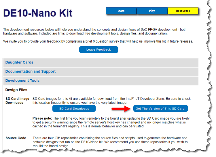
5. Your web browser will display a text string that looks something like this:

6. The last part of the string, highlighted above, contains the date the SD Card image was built. In this example it reports a build date of March 22, 2017. The Mandelbrot design is included in all versions built in 2018 and later.
- Where Do I Get the Mandelbrot Design?
-
- Go to the Downloads for the Terasic DE10-Nano Kit page here.
- Download the latest release.
- Update your microSD Card with the new image. Instructions are located here.
Board Connections and Setup
1. Make sure the microSD Card is inserted in the board.
2. Connect the Terasic DE10-Nano board HDMI output to the monitor using an HDMI cable.
3. Set slide switches SW3 to SW0 to "0001" as shown below:
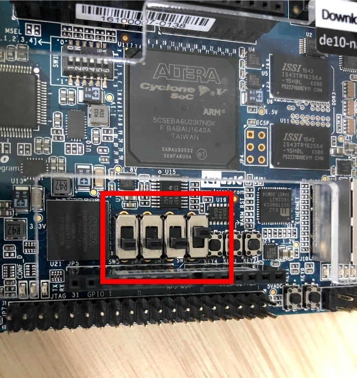
Figure 4. Slide Switch Settings (SW3 – SW0)
4. Apply power to the HDMI monitor.
5. Apply power to the Terasic DE10-Nano board by connecting the power adapter and plugging the power cable (DC 5V) into a wall outlet.
Initial Operation
After the board boots, it will begin displaying fractal images on the monitor. The application chooses various points within the image, zooms in to reveal more detail, zooms out, picks a new point, then repeats. By default, the board uses the Mandelbrot Engine in the FPGA fabric to generate the fractal images. Image data generated by the Mandelbrot Engine is written to a buffer in the external SDRAM, then read by the video pipeline and sent to the HDMI interface.
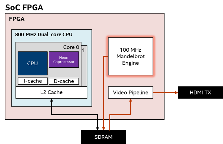
Figure 5. Block Diagram – FPGA Operation
1. Notice the information displayed at the bottom left corner of the screen:
- FPS: Shows the number of frames per second being generated.
- Algo: Shows the method being used to generate the images; HW algo (FPGA) or SW algo (CPU).
- %CPU: Shows the percentage of CPU bandwidth being used to generate the images.
2. Notice the scrolling text in the bottom right corner of the display:
- Provides details about the algorithm that is running.
- Gives instructions on how to open the menu.
- Gives instruction on how to switch between HW and SW operation.
3. Switch to CPU operation by pressing the push button labeled KEY1.
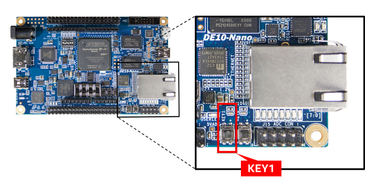
Figure 6. Location of push button KEY1
The fractal images are now being generated by the dual-core Arm Cortex-A9 CPU. Image data generated by the CPU is written to the buffer in the external SDRAM, then read by the video pipeline and sent to the HDMI interface.
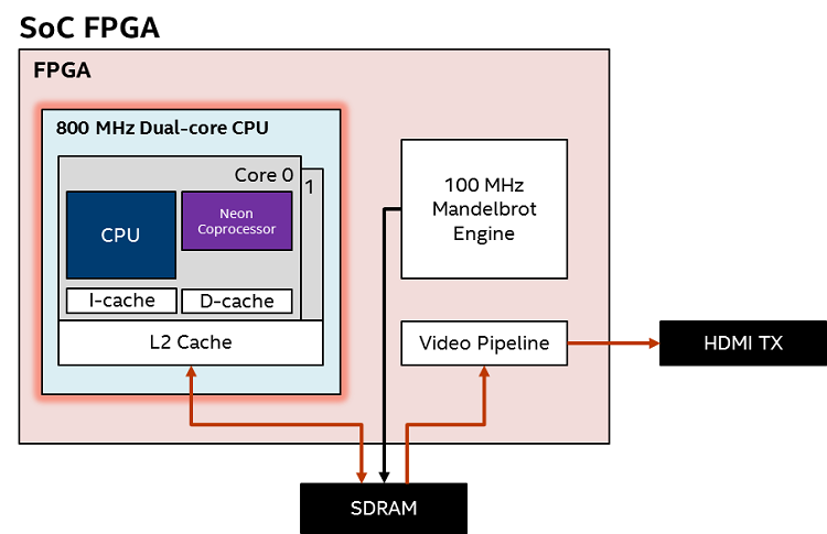
Figure 7. Block Diagram – CPU Operation
4. Note the performance (FPS) and CPU usage (%CPU) displayed in the bottom left corner of the display.
5. Toggle between FPGA and CPU operation by pressing KEY1.
Notice how the display is updated faster (more FPS), and with a low %CPU utilization (~ 4% to 6%) in FPGA operation.
Notice how much slower the display is updated when using the CPU. Also notice that the %CPU utilization is 99% or greater, fulling consuming the CPU processing resources. This illustrated two key virtues of using FPGAs for complex algorithms:
- FPGAs are faster. Even though it is running at a lower clock frequency than the CPU (100MHz vs 800MHz in this example) the FPGA outperforms the CPU. This is because of the parallel nature of FPGAs, and their ability to generate a result on every clock cycle, or create computation pipelines which keep each stage of the pipeline busy on every clock cycle performing work for different operations that are required.
Processors execute tasks sequentially, one instruction at a time. Depending on the processor architecture, each instruction can take several CPU clock cycles to complete. Execution time also depends on how fast the CPU can access memory for instructions and data.
The Cyclone® V SoC FPGA used in this design is optimized for cost, not performance. Imagine how much faster the algorithm would run in a device optimized for performance like Intel® Stratix® 10 FPGA and Intel® Arria® 10 FPGA and Intel® SoC FPGA.
- FPGAs can off-load CPUs from complex algorithms freeing them for other tasks, like running a network stack, managing a file system, or interfacing with other board resources. It lets the CPU do more of what it does best.
Using the Menus
Software running on the processor lets you modify how the system operates. You can open the Main Menu from which you can access several sub-menus to change settings. Here are the sub-menus available:
- Configure Continuous Demo: Lets you change how the processing is performed for both FPGA and CPU operation, and how the display is updated.
- Algorithm Performance: Measures the performance of processing methods you have selected.
- Algorithm Accuracy: Compares the accuracy of the algorithms when run in integer and floating-point modes.
- Explore: Lets you pick points on the display and zoom in. It uses the board’s accelerometer like a mouse to move a cursor around the display.
- About Demo: Get details about this design.
- Reboot: Reboot the board.
- Power off: Orderly shut-down of the board (recommended).
Let’s get started!
1. Bring up the "Main Menu" by pressing the push button labeled "KEY0" on your Terasic DE10-Nano Development Kit.
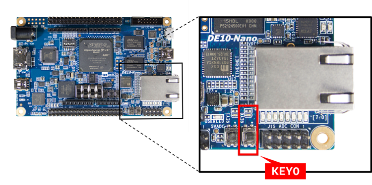
Figure 8. Terasic DE10-Nano Development Kit "Key 0" Button
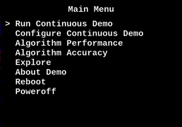
Figure 9. Mandelbrot Demo: "Main Menu"
2. Scroll to the About Demo choice by pressing KEY1 on your Terasic DE10-Nano Development Kit.
3. Select this option by pressing KEY0.
4. Read details about the design, advancing through the text display by pressing either key. Contained within the text are the compiler version, options, and libraries used to create the software, as well as the Intel® Quartus® Prime Software version used to generate the FPGA hardware design.
5. When you return to the Main Menu, press KEY0 to Run Continuous Demo.
Now that you know how to navigate the menus, let’s explore the rest of this application.
Algorithm Performance Metrics
We saw how much faster the FPGA generated images than the CPU, but let’s measure the actual time it takes. Here’s how:
1. Press KEY0 to open the Main Menu.
2. Select the Algorithm Performance choice.
3. Choose Software Algorithm Performance.
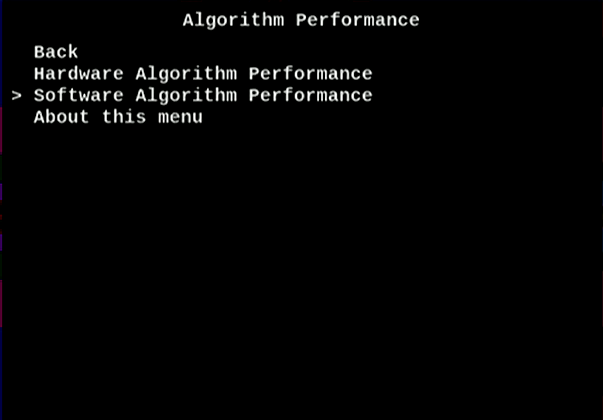
Figure 10. Software Algorithm Performance
4. Select Multithreaded Cortex A9 NEON FP VI. This is the highest performance configuration for the CPU.
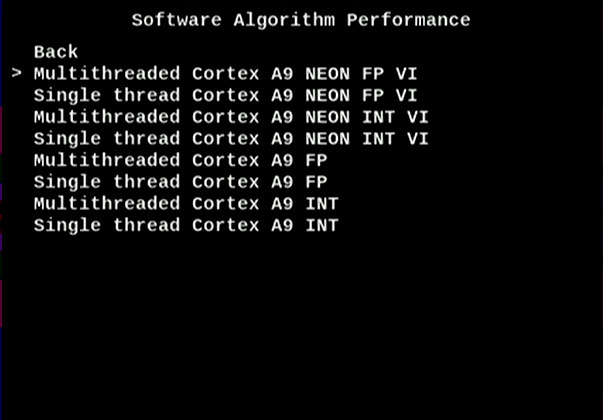
Figure 11. Multithreaded Cortex A9 NEON FP VI Performance
Software running on the dual-core Arm Cortex-A9 processor in the Cyclone V SoC FPGA device can be configured to operate in one of eight modes using any combination of the following choices:
- Single thread / Multithreaded: Runs code as a single thread, or multiple threads.
- INT / FP: Uses integer or floating-point arithmetic.
- NEON VI / : NEON VI indicates optimized code targeting the NEON* coprocessor. NEON vector intrinsics are special instructions set extensions for the NEON coprocessor which provide Single Instruction Multiple Data (SIMD) capabilities. Options without "NEON VI" in the name represent standard C code targeting the Arm CPU.
The algorithm is run by the dual-core CPU (plus NEON* coprocessor) generating an image in just under 220ms. Your results may vary slightly.
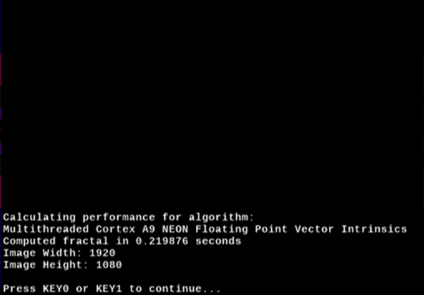
Figure 12. Software Algorithm Performance – Multithreaded, Floating Point, NEON VI
5. Press KEY0 or KEY1 to continue, then select Back.
6. Choose Hardware Algorithm Performance, then select FPGA (12 accelerator).
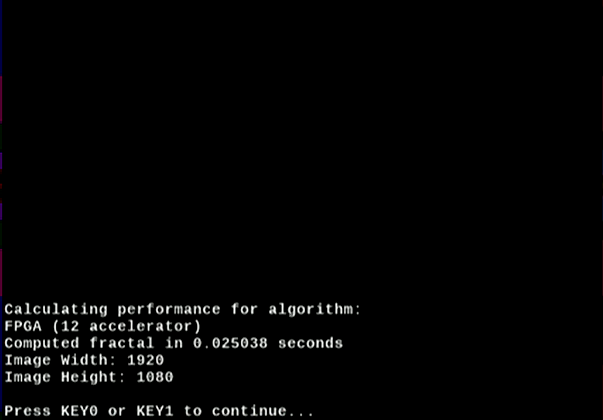
Figure 13. Hardware Algorithm Performance – 12 accelerators
The algorithm is run in the FPGA using 12 accelerators, generating the image in just over 25ms. This is over 8 times faster than the CPU.
6. Experiment with other operating settings and see how fast they are.
7. Return to the continuous demo.
Modify FPGA Hardware Settings
This menu lets you select the number of accelerator cores used by the Mandelbrot engine in the FPGA. You can choose from 1 to 12 accelerators to work in parallel. By default, the system uses all 12 cores.
1. Press KEY0 to open the Main Menu.
2. Select the Continuous Demo Configuration choice.
3. Select Configure Hardware Algorithm.
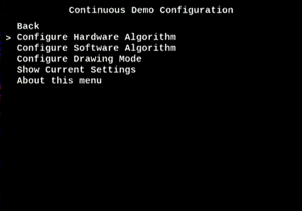
Figure 14. Configure Hardware Algorithm
- How Does the Mandelbrot Engine Work?
-
Custom hardware implemented in the FPGA performs Mandelbrot calculations to generate the fractal images.
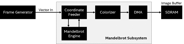
Figure 15. FPGA Mandelbrot Subsystem Block DiagramA frame generator feeds image vectors into a Mandelbrot subsystem. The vectors are converted to coordinates which are fed to the Mandelbrot engine. The output is them colored based on how close the coordinate is to being within the Mandelbrot set, and a DMA transfers the pixel data to the image buffer in external SDRAM.
The subsystem above produces images very quickly, but to get even more performance, multiple sub-systems are combined and operate in parallel to achieve even higher performance.
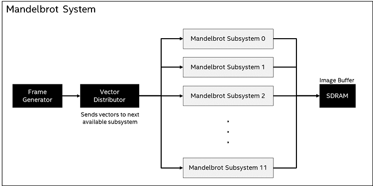
Figure 16. FPGA Mandelbrot System Block DiagramA Vector Distributor is used to send vectors to the next available subsystem, making sure that all are continually processing vectors, and writing pixel data to the image buffer in SDRAM.
From the menu system provided in this design, you can choose how many Mandelbrot subsystems (acceleration cores) are used.
4. Select 1 Mandelbrot core - FPGA (1 accelerator) - from the menu.
5. Select Back, then choose Run Continuous Demo and watch the speed of the images being drawn.
6. Toggle between HW algo and SW algo by pressing KEY1, and notice the performance difference. FPGA operation is a little slower than the CPU when only 1 accelerator is used, but CPU operation still requires 100% of the CPU bandwidth.
7. Experiment with the number of accelerators to see where the FPGA and CPU run at about the same speed.
8. When you are done, configure the hardware algorithm to use 12 accelerators.
Modify CPU Software Settings
By default, software operation (SW algo) is configured to run on the dual-core Arm Cortex-A9 processor using the fastest configuration:
- Multithreaded operation
- NEON coprocessor enabled
- Uses floating point vector intrinsic instruction set extensions
Let’s experiment with some of the other settings.
1. Press KEY0 to open the Main Menu.
2. Select the Continuous Demo Configuration choice.
3. Select Configure Software Algorithm.
4. Choose Single Thread Cortex A9 NEON FP VI.
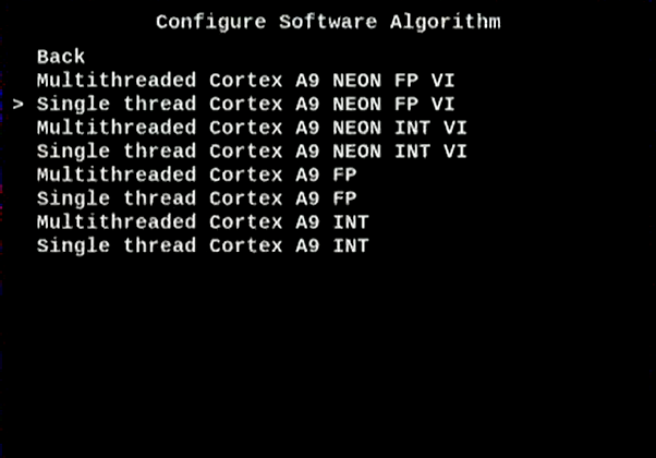
Figure 17. Configure Software Algorithm
5. Select Back, then Run Continuous Demo.
6. Press KEY1 to switch to software operation (SW algo).
7. Notice the performance metrics. Frames per second (FPS) are reduced significantly, but the %CPU usage is reduced as well (~ 55%).
You can choose other configuration options to see how they impact the performance (FPS and %CPU utilization). Some other interesting choices to try are:
- Multithreaded Cortex A9 FP (without the NEON coprocessor)
- Single thread Cortex A9 INT
Note: You can see which operating mode is being used by watching the scrolling text in the lower right corner of the display.
8. When you are done experimenting, configure the Software Algorithm to use Multithreaded Cortex A9 NEON FP VI and put it back in Run Continuous Demo mode.
Modify the Drawing Mode
We can also change the way the images are sent to the monitor. This alters the way the image buffer in the SDRAM is used. There are two choices you can make:
- Draw directly into a live frame buffer
With this choice enabled you can see the screen being updated in real time as image data is written into the frame buffer. - Draw into a buffered frame buffer (default)
With this choice enabled display the display is not updated until a complete image has been written to the frame buffer.
- How Does the Frame Buffer Work?
-
Once image data has been written to the SDRAM, the video pipeline reads the data out using an internal DMA, and sends it to the HDMI interface chip using the proper clocking.
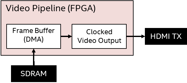
Figure 18. FPGA Video Pipeline Block DiagramImage data stored in SDRAM can be organized in one of two ways:
1. Direct (or "live buffer") – As data is written into the image buffer, data is also being read out of the buffer and send to the display. If the image data is being generated slowly enough you can see the image being updated line by line.
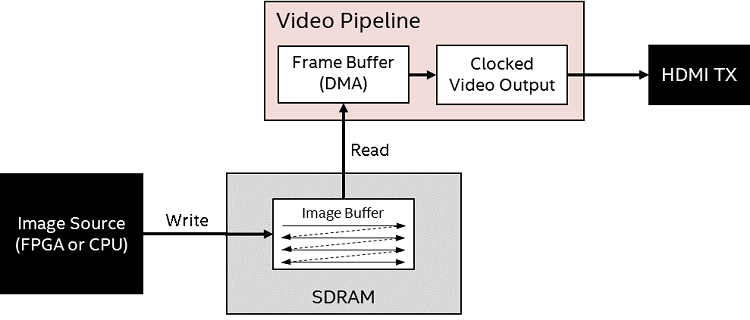
Figure 19. Direct Image Buffer Operation Block Diagram2. Buffered (or "ping-pong") – In this mode three buffers are used. One is always being written to, and one is always being read from. The third buffer exists because the point in time when a new image has been generated (written), doesn’t always align with the time the previous image has been displayed (read). With three buffers there is always a place for a new image to go, and the video pipeline can always read from the last complete image if a new image isn’t ready.
Software controls which buffer is being written to, and read from. In this mode, the monitor is updated with a complete image every time.
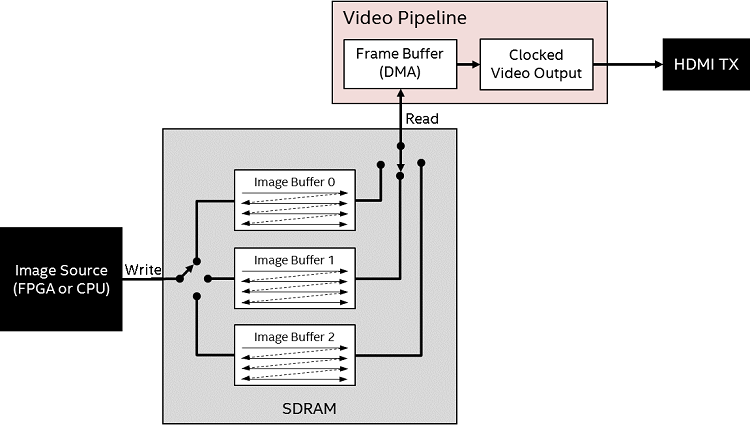
Figure 20. Buffered Operation Block Diagram
- Press KEY0 to open the Main Menu.
- Select the Continuous Demo Configuration choice.
- Choose Configure Drawing Mode.
- Select Draw directly into live frame buffer.
- Select Back, then choose Run Continuous Demo.
- Switch to CPU operation by pressing KEY1 and it will be easier to see the speed at which the CPU writes the image data to the frame buffer.
- You can leave the display in this mode or switch back to the buffered (default) mode to suit your tastes.
Exploring the Mandelbrot Image
The "Explore" mode lets you choose a part of the image to view in more detail. In this mode a cursor appears that you position using the on-board accelerometer, tipping the board from side to side or front to back to move it.
- Make sure the Terasic DE10-Nano board is on a flat, level surface.
- Press KEY0 to open the Main Menu.
- Choose Explore.
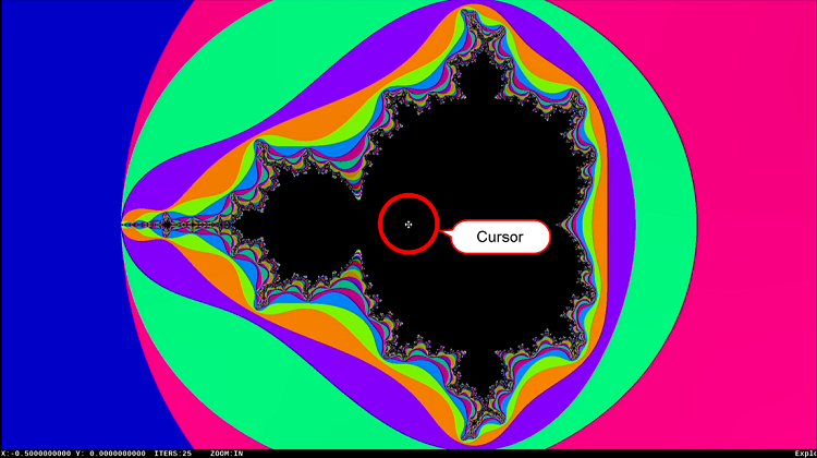
Figure 21. Mandelbrot Demo: "Explore Menu"
4. Notice the cursor.
5. Tilt the board to move the cursor to any place on the display where you wish to see more detail (i.e. zoom in).
6. Put the board back to level then press KEY1 to zoom in. At some point you will notice that you aren’t getting much more detail. That is because the number of iterations is set too low.
7. Press KEY0 to re-open Explore Menu.
8. Select Change iteration count.
9. Choose a larger count – like 100.
10. Press KEY0 to Close the menu.
11. Continue to zoom in by pressing KEY1. You will now see much more detail when you zoom in.
12. When you are done exploring, press KEY0 to re-open the Explore Menu.
13. Select Exit Explore Mode.
14. Choose Run Continuous Demo.
Algorithm Accuracy
The Algorithm Accuracy menu lets you compare the mathematical accuracy between the various operating modes:
- Integer with floating-point
Compares the accuracy between the integer and floating-point algorithms for a full frame of the Mandelbrot calculation. Due to the different precision of floating point and integer arithmetic we expect differences between a full-frame integer and full-frame floating point computation. - All floating-point algorithms
Compares the accuracy between the floating-point algorithms (single threaded, multi-threaded, NEON vector intrinsic). Since the precision is the same for all floating-point computations we expect no differences between them. - All integer algorithms
Compares the accuracy between the integer algorithms (single threaded, multi-threaded, NEON). Since the precision is the same for all integer computations we expect no differences between them.
1. Press KEY0 to open the Main Menu.
2. Choose Algorithm Accuracy.
3. Select Compare integer with floating point.
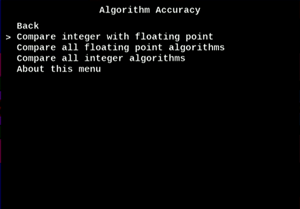
Figure 22. Compare Floating-point to Integer
The results are calculated and displayed as shown below. In this test, we expect to see differences in the results due to the different precision characteristics of floating-point and integer arithmetic.
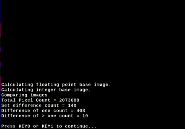
Figure 23. Accuracy Results - Compare Floating-point to Integer
4. Press either KEY0 or KEY1 to continue.
5. Try one of the other choices (i.e. all floating-point, or all integer).
6. Return to the continuous demo.
Power Off
When you’re done playing with the DE10-Nano board we recommend you shut it off as follows:
- Press KEY0 to open the Main Menu.
- Choose Poweroff.
- Disconnect the power cable
You can always just pull the power plug, but since the system is running Linux*, shutting it down improperly may leave remnants on the SDCard.
"