The Intel® Xeon® processor D-2100 product family, formerly code named Skylake-D, is Intel's latest generation 64-bit server system-on-chip (SoC). It is manufactured using the Intel low-power SoC 14 nm process, with up to 18 cores, and from 60 to 110 watts of power consumption. It brings the architectural innovations from the Intel® Xeon® Scalable processor platform to an SoC processor.

Figure 1. Comparison of server and microserver product lines.
In Intel's product line the Intel Xeon D processor is positioned between the Intel Xeon Scalable processor, which is focused on server-level performance and the Intel Atom® processor 3000, which is focused on providing the lowest power of the three product lines. The Intel Xeon processor D-2100 product family provides lower power than the Intel Xeon Scalable processor product family and higher performance than the Intel Atom processor C3000 product family.
Table 1.Summary of segments that can benefit from the Intel® Xeon® processor D-2100 product family.
| Business Processing |
Cloud Services |
Visualization & Audio |
Communication |
Storage |
|---|---|---|---|---|
| Dynamic Web Serving |
Dynamic Front End Web |
Media Delivery and Transcode |
Wired Networking |
Scale-Out/ Distributed DB |
| File & Print |
Memory Caching |
Edge Routing |
Warm Cloud/Object Storage |
|
| Active-Archive |
||||
| Dedicated Hosting |
Edge Security / Firewall |
Enterprise SAN/NAS |
||
| Virtual Switching |
Cold Storage Backup/Disaster Recovery |
|||
| Wireless Base Station |
The Intel Xeon processor D-2100 product family is optimized for parallel software that benefits mostly from more individual servers with sufficient input/output (I/O) between nodes including dynamic web servers, hot or cold storage, network routing, enterprise storage area network/network attached storage (SAN/NAS), virtual switching, edge firewall security, wireless LAN controllers, distributed memory caching (memcached), distributed database, and any of the aforementioned uses that have an additional need for acceleration of cryptographic communications such as security appliances and switches.
Typically, the Intel Xeon processor D-2100 product family will be found populating a microserver chassis, which is comprised of multiple Intel Xeon SoC D-2100 product family nodes sharing a common chassis, fans, and power supplies, and is interconnected to achieve improved flexibility, higher efficiency, and optimization of rack density. Microservers based on Intel Xeon SoC D-2100 product family nodes can meet different usage models, such as combining with lots of disk storage to provide a hot storage solution, or to provide a low power, high density network solution.
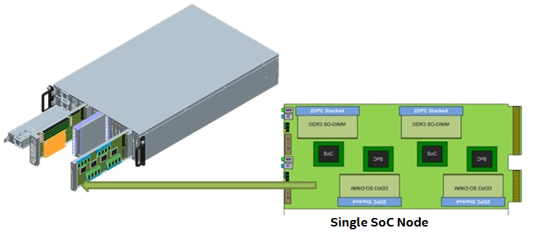
Figure 2. Generic, high-level overview of how a microserver chassis is composed of multiple SoC nodes, along with shared components (such as power supply, fans, and chassis).
There are three separate product SKUs for the Intel Xeon processor D-2100 product family. When the processor model number ends in the letter "I", the SKUs are more focused on computation and cloud segments. Model numbers ending in "IT" are associated with network and enterprise storage segments. And model numbers ending in "NT" include Integrated Intel® QuickAssist Technology (Intel® QAT) to help with acceleration of cryptographic workloads. To see a list of the processor models with more specifications, see the Intel Xeon processor D-2100 product family brief.
SoC Architecture Overview
Table 2. Provides a high-level summary of the hardware differences between the Intel® Xeon® processor D-2100 product family and the Intel Xeon processor D-1500 product family.
| Intel® Xeon® SoC D-1500 |
Intel® Xeon SoC D-2100 |
|
|---|---|---|
| Thermal Design Point (TDP) |
20–65W |
60–110W |
| Cores |
Up to 16C with Intel® Hyper-Threading Technology (Intel® HT Technology) |
Up to 18C with Intel® HT Technology |
| Micro-Architecture |
Broadwell |
Skylake |
| Package Size |
37.5mm x 37.5mm |
45mm x 52.5mm |
| Key Target |
Network/Storage/Compute |
Storage/Compute/Network |
| Intel® Advanced Vector Extensions (Intel® AVX) |
Intel® Advanced Vector Extensions 2 (Intel® AVX2) |
Intel® Advanced Vector Extensions 512 (Intel® AVX-512) New Instructions |
| Cache |
LLC: 1.5MB/core |
LLC: 1.375MB/core |
| MLC: 256k/core |
MLC: 1MB/core |
|
| Memory |
2 channels DDR4 2400 MHz per SoC Up to 128G memory capacity |
4 channels† DDR4 2666 MHz per SoC Up to 512GB memory capacity |
| Ethernet |
Up to four 10GbE/1GbE ports |
Up to four 10GbE/1GbE ports with accelerated Remote Direct Memory Access (RDMA) and native Software Fault Isolation (SFI) |
| PCIe† |
PCIe 3.0 (2.5, 5.0, 8.0 GT/s) |
PCIe 3.0 (2.5, 5.0, 8.0 GT/s) |
| 32 Gen3 lanes + Up to 20 Gen3 (through Flexible High Speed I/O) |
32 Gen3 lanes + Up to 20 Gen3 (through Flexible High Speed I/O) |
|
| SATA |
6 SATA ports |
Up to: 14 SATA (through Flexible High Speed I/O) |
| Integrated Crypto / Encrypt / Decrypt Offload Acceleration |
Integrated Intel® QuickAssist Technology (Intel® QAT): Up to 40G Crypto/20G Compression, 40kOps Public Key Encryption (PKE) 2K |
Integrated Intel QAT: Up to 100G Crypto/Compression + 100kOps Public Key Encryption (PKE) 2K |
New capabilities relative to previous generations vary with SKUs.
The Intel Xeon processor D-2100 product family is a new microarchitecture with many additional features compared to the previous-generation of the Intel Xeon processor D-1500 product family (formerly Broadwell microarchitecture). These features include increased processor cores, increased memory channels, a non-inclusive cache, Intel® AVX-512, Intel® Memory Protection Extensions (Intel® MPX), Intel® Speed Shift Technology, and Internet Wide Area RDMA Protocol (iWARP). A flexible I/O interface provides up to 20 configurable high-speed lanes that allow original equipment manufacturers (OEMs) the ability to make customized I/O choices for the baseboard. The rest of this paper will cover these various technologies in greater detail.
Table 3. Overview of product technologies for the Intel® Xeon® processor D-2100 product family.
| Product Technology | |
|---|---|
| Intel Xeon Mesh Architecture | Iwarp RDMA |
| Cache Hierarchy Changes | RAS |
| Intel® MPX | Intel® Volume Management Device (Intel® VMD) |
| Mode based Execution Control (XU/XS bits) | Intel® Platform Storage Extensions |
| Intel® AVX-512 | Intel® Boot Guard |
| Intel® Speed Shift Technology and PMax | Innovation Engine |
| Intel® QuickAssist Technology (Intel® QAT) | Intel® Node Manager (Intel® NM) |
Intel® Xeon® mesh architecture
On the previous generation of Intel Xeon D processor the cores, last-level cache (LLC), memory controller, I/O controller, and inter-socket pathways are connected using a ring architecture. This ring architecture has been around for many years on the different product lines offered by Intel.
The Intel Xeon SoC D-2100 product family has advanced beyond the ring architecture, introducing a new mesh architecture to mitigate the increased latencies and bandwidth constraints associated with previous ring architecture. The mesh architecture encompasses an array of vertical and horizontal communication paths allowing traversal from one core to another through a shortest path (hop on vertical path to correct row, and hop across horizontal path to correct column). The caching and home agent (CHA) located at each of the LLC slices maps addresses being accessed to a specific LLC bank, memory controller, or I/O subsystem, and provides the routing information required to reach its destination using the mesh interconnect.
In addition to the improvements expected in the overall core-to-cache and core-to-memory latency, we also expect to see improvements in latency for I/O-initiated accesses. In the previous generation of processors, in order to access data in LLC, memory, or I/O, a core or I/O would need to go around the ring. In the Intel Xeon SoC D-2100 product family, a core or I/O can access the data in LLC, memory, or I/O through the shortest path over the mesh.
Cache hierarchy changes
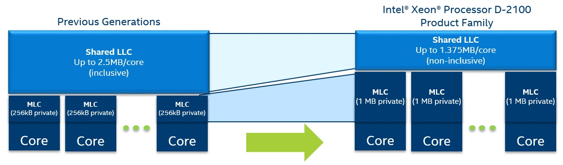
Figure 3. Generational cache comparison.
In the previous generation, the mid-level cache was 256 KB per core and the Last-Level Cache (LLC) was a shared inclusive cache, with 1.5 MB per core. In the Intel Xeon processor D-2100 product family, the cache hierarchy has changed to provide a larger Mid-Level Cache (MLC) of 1 MB per core and a smaller, shared non-inclusive 1.375 MB LLC per core. A larger MLC increases the hit rate into the MLC resulting in lower effective memory latency and also lowers demand on the mesh interconnect and LLC. The shift to a non-inclusive cache for the LLC allows for more effective utilization of the overall cache on the chip versus an inclusive cache.
If the core on the Intel Xeon processor D-2100 product family has a miss on all the levels of the cache, it fetches the line from memory and puts it directly into MLC of the requesting core, rather than putting a copy into both the MLC and LLC, as was done on the previous generation. When the cache line is evicted from the MLC it is placed into the LLC if it is expected to be reused.
Due to the non-inclusive nature of LLC, the absence of a cache line in LLC does not indicate that the line is not present in private caches of any of the cores. Therefore, a snoop filter is used to keep track of the location of cache lines in the L1 or MLC of cores when it is not allocated in the LLC. On previous-generation CPUs, the shared LLC itself took care of this task.
Even with the changed cache hierarchy in the Intel Xeon processor D-2100 product family, the effective cache available per core is roughly the same as the previous generation for a usage scenario where different applications are running on different cores. Because of the non-inclusive nature of LLC, the effective cache capacity for an application running on a single core is a combination of MLC cache size and a portion of LLC cache size. For other usage scenarios, such as multithreaded applications running across multiple cores with some shared code and data, or a scenario where only a subset of the cores on the socket are used, the effective cache capacity seen by the applications may seem different than previous-generation CPUs. In some cases, application developers may need to adapt their code to optimize it with the change in the cache hierarchy.
Intel® Memory Protection Extensions (Intel® MPX)
C/C++ pointer arithmetic is a convenient language construct often used to step through an array of data structures. If an iterative write operation does not take into consideration the bounds of the destination, adjacent memory locations may get corrupted. Such unintended modification of adjacent data is referred to as a buffer overflow. Buffer overflows have been known to be exploited, causing denial-of-service attacks and system crashes. Similarly, uncontrolled reads could reveal cryptographic keys and passwords. More sinister attacks that do not immediately draw the attention of the user or system administrator alter the code execution path, such as modifying the return address in the stack frame to execute malicious code or script.
Intel's Execute Disable Bit and similar hardware features from other vendors have blocked buffer overflow attacks that redirected the execution to malicious code stored as data. Intel MPX technology consists of new Intel® architecture instructions and registers that compilers can use to check the bounds of a pointer at runtime before it is used. This new hardware technology is supported by the compiler.
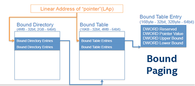
Figure 4. New Intel MPX instructions and example of their effect on memory.
| New Instruction | Function |
|---|---|
| BNDMK b, m | Creates LowerBound (LB) and UpperBound (UB) in bounds register b. |
| BNDCL b, r/m | Checks the address of a memory reference or address in r against the lower bound. |
| BNDCU b, r/m | Checks the address of a memory reference or address in r against the upper bound. |
| BNDCN b, r/m | Checks the address of a memory reference or address in r against the upper bound in one's compliment. |
For additional information see the Intel Memory Protection Extensions Enabling Guide.
Mode-based execute control
Mode-based execute provides finer grain control on execute permissions to help protect the integrity of the system code from malicious changes. It provides additional refinement within the extended page tables by turning the Execute Enable (X) permission bit into two options:
- XU for user pages
- XS for supervisor pages
The CPU selects one or the other based on permission of the guest page and maintains an invariant for every page that does not allow it to be writable and supervisor-executable at the same time. A benefit of this feature is that a hypervisor can more reliably verify and enforce the integrity of kernel-level code. The value of the XU/XS bits is delivered through the hypervisor, so hypervisor support is necessary.
Intel® Advanced Vector Extensions 512 (Intel® AVX-512)
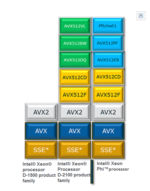
Figure 5. Generational overview of Intel® AVX technology.
Intel® AVX-512 was originally introduced with the Intel® Xeon Phi™ processor product line. There are certain Intel AVX-512 instruction groups (AVX512CD and AVX512F) that are common to the Intel Xeon Phi processor product line and the Intel Xeon processor D-2100 product family. However, the Intel Xeon processor D-2100 product family introduces new Intel AVX-512 instruction groups (AVX512BW and AVX512DQ), as well as a new capability (AVX512VL) to expand the benefits of the technology. The AVX512DQ instruction group is focused on new additions for benefiting high-performance computing (HPC) workloads such as oil and gas, seismic modeling, the financial services industry, molecular dynamics, ray tracing, double-precision matrix multiplication, fast Fourier transform and convolutions, and RSA cryptography. The AVX512BW instruction group supports Byte/Word operations, which can benefit some enterprise applications and media applications, as well as HPC. AVX512VL is not an instruction group but a feature that is associated with vector length orthogonality.
Feature list of the Intel® AVX-512 technology.
- One 512-bit FMA
- 512-bit FP and Integer
- 32 registers
- 8 mask registers
- 32 SP/16 DP Flops/Cycle
- Embedded rounding
- Embedded broadcast
- Scalar / SSE / Intel AVX "promotions"
- Native media additions
- HPC additions
- Transcendental support
- Gather/Scatter
Intel AVX-512 instructions offer the highest degree of support to software developers by including an unprecedented level of richness in the design of the instructions. This includes 512-bit operations on packed floating-point data or packed integer data, embedded rounding controls (override global settings), embedded broadcast, embedded floating-point fault suppression, embedded memory fault suppression, additional gather/scatter support, high-speed math instructions, and compact representation of large displacement value. The following sections cover some of the details of the new features of Intel AVX-512.
AVX512DQ
The doubleword and quadword instructions, indicated by the AVX512DQ CPUID flag enhance integer and floating-point operations, consisting of additional instructions that operate on 512-bit vectors whose elements are 16 32-bit elements or 8 64-bit elements. Some of these instructions provide new functionality such as the conversion of floating-point numbers to 64-bit integers. Other instructions promote existing instructions such as with the vxorps instruction to use 512-bit registers.
AVX512BW
The byte and word instructions, indicated by the AVX512BW CPUID flag, enhance integer operations, extending write-masking and zero-masking to support smaller element sizes. The original Intel AVX-512 foundation instructions supported such masking with vector element sizes of 32 or 64 bits because a 512-bit vector register could hold at most 16 32-bit elements, so a write mask size of 16 bits was sufficient.
An instruction indicated by an AVX512BW CPUID flag requires a write mask size of up to 64 bits because a 512-bit vector register can hold 64 8-bit elements or 32 16-bit elements. Two new mask types (_mmask32 and _mmask64) along with additional maskable intrinsics have been introduced to support this operation.
AVX512VL
An additional orthogonal capability known as vector length extensions provide for most Intel AVX-512 instructions to operate on 128 or 256 bits, instead of only 512. Vector length extensions can currently be applied to most foundation instructions and the conflict detection instructions, as well as the new byte, word, doubleword, and quadword instructions. These Intel AVX-512 vector length extensions are indicated by the AVX512VL CPUID flag. The use of vector length extensions extends most Intel AVX-512 operations to also operate on XMM (128-bit, SSE) registers and YMM (256-bit, Intel® AVX) registers. The use of vector length extensions allows the capabilities of EVEX encodings including the use of mask registers and access to registers 16..31 to be applied to XMM and YMM registers, instead of only to ZMM registers.
Mask registers
In previous generations of Intel AVX and Intel® AVX2 the ability to mask bits was limited to load and store operations. In Intel AVX-512, this feature has been greatly expanded with eight new opmask registers used for conditional execution and efficient merging of destination operands. The width of each opmask register is 64 bits, and they are identified as k0–k7. Seven of the eight opmask registers (k1–k7) can be used in conjunction with EVEX-encoded Intel AVX-512 foundation instructions to provide conditional processing, such as with vectorized remainders that only partially fill the register, while the opmask register k0 is typically treated as a "no mask" when unconditional processing of all data elements is desired. Additionally, the opmask registers are also used as vector flags/element level vector sources to introduce novel SIMD functionality, as seen in new instructions such as VCOMPRESSPS. Support for the 512-bit SIMD registers and the opmask registers is managed by the operating system using XSAVE/XRSTOR/XSAVEOPT instructions (see Intel® 64 and IA-32 Architectures Software Developer's Manual, Volume 2B, and Intel® 64 and IA-32 Architectures Software Developer's Manual, Volume 3A).
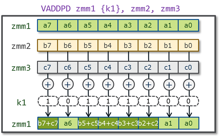
Figure 6. Example of opmask register k1.
Embedded rounding
Embedded rounding provides additional support for math calculations by allowing the floating-point rounding mode to be explicitly specified for an individual operation, without having to modify the rounding controls in the MXCSR control register. In previous SIMD instruction extensions, rounding control is generally specified in the MXCSR control register, with a handful of instructions providing per-instruction rounding override via encoding fields within the imm8 operand. Intel AVX-512 offers a more flexible encoding attribute to override MXCSR-based rounding control for floating-point instruction with rounding semantics. This rounding attribute embedded in the EVEX prefix is called Static (per instruction) Rounding Mode or Rounding Mode Override. Static rounding also implies exception suppression (SAE) as if all floating-point exceptions are disabled and no status flags are set. Static rounding enables better accuracy control in intermediate steps for division and square root operations for extra precision, while the default MXCSR rounding mode is used in the last step. It can also help in cases where precision is needed for the least significant bit such as in range reduction for trigonometric functions.
Embedded broadcast
Embedded broadcast provides a bit field to encode data broadcast for some load-op instructions, such as instructions that load data from memory and perform some computational or data movement operation. A source element from memory can be broadcasted (repeated) across all elements of the effective source operand without requiring an extra instruction. This is useful when we want to reuse the same scalar operand for all operations in a vector instruction. Embedded broadcast is only enabled on instructions with an element size of 32 or 64 bits, and not on byte and word instructions.
Quadword integer arithmetic
Quadword integer arithmetic removes the need for expensive software emulation sequences. These instructions include gather/scatter with D/Qword indices, and instructions that can partially execute, where k-reg mask is used as a completion mask.
Table 4. Quadword integer arithmetic instructions.
| Instruction | Description |
|---|---|
| VPADDQ zmm1 {k1}, zmm2, zmm3 | INT64 addition |
| VPSUBQ zmm1 {k1}, zmm2, zmm3 | INT64 subtraction |
| VP{SRA,SRL,SLL}Q zmm1 {k1}, zmm2, imm8 | INT64 shift (imm8) |
| VP{SRA,SRL,SLL}VQ zmm1 {k1}, zmm2, zmm3 | INT64 shift (variable) |
| VP{MAX,MIN}Q zmm1 {k1}, zmm2, zmm3 | INT64 max, min |
| VP{MAX,MIN}UQ zmm1 {k1}, zmm2, zmm3 | INT64 max, min |
| VPABSQ zmm1 {k1}, zmm2, zmm3 | INT64 absolute value |
| VPMUL{DQ,UDQ} zmm1 {k1}, zmm2, zmm3 | 32x32 = 64 integer multiply |
Math support
Math support is designed to aid with math library writing and to benefit financial applications. Data types that are available include PS, PD, and SS. IEEE division/square root formats, DP transcendental primitives, and new transcendental support instructions are also included.
Table 5. A portion of the 30 math support instructions.
| Instruction |
Description |
|---|---|
| VGETXEP {PS,PD,SS,SD} |
Obtain exponent in FP format |
| VGETMANT {PS,PD,SS,SD} |
Obtain normalized mantissa |
| VRNDSCALE {PS,PD,SS,SD} |
Round to scaled integral number |
| VFIXUPIMM {PS,PD,SS,SD} |
Patch output numbers based on inputs |
| VRCP14 {PS,PD,SS,SD} |
Approx. reciprocal() with rel. error 2-14 |
| VRSQRT14 {PS,PD,SS,SD} |
Approx. rsqrt() with rel. error 2-14 |
| VDIV {PS,PD,SS,SD} |
IEEE division |
| VSQRT {PS,PD,SS,SD} |
IEEE square root |
New permutation primitives
Intel AVX-512 introduces new permutation primitives, such as two-source shuffles with 16/32-entry table lookups with transcendental support, matrix transpose, and a variable VALIGN emulation.
Table 6. Two-source shuffles instructions
| 2-Src Shuffles |
|---|
| VSHUF{PS,PD} |
| VPUNPCK{H,L}{DQ,QDQ} |
| VUNPCK{H,L}{PS,PD} |
| VPERM{I,D}2{D,Q,PS,PD} |
| VSHUF{F,I}32X4 |
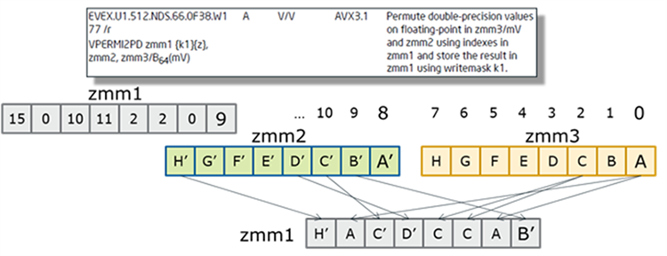
Figure 7. Example of a two-source shuffles operation.
Expand and compress
Expand and compress allows vectorization of conditional loops. Similar to Fortran pack/unpack intrinsic, it also provides memory fault suppression, can be faster than using gather/scatter, and also has opposite operation capability for compress. The figure below shows an example of an expand operation.
VEXPANDPS zmm0 {k2}, [rax]
Moves compressed (consecutive) elements in register or memory to sparse elements in register (controlled by mask), with merging or zeroing.
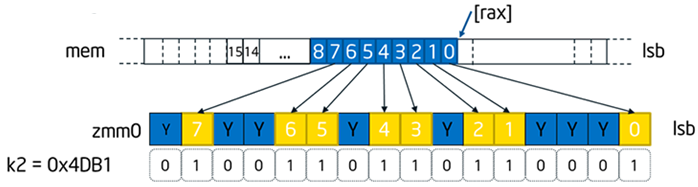
Figure 8. Expand instruction and diagram.
Bit Manipulation
Intel AVX-512 provides support for bit manipulation operations on mask and vector operands including vector rotate. These operations can be used to manipulate mask registers, and they have some application with cryptography algorithms.
Table 7. Bit manipulation instructions.
| Instruction |
Description |
|---|---|
| KUNPCKBW k1, k2, k3 |
Interleave bytes in k2 and k3 |
| KSHIFT{L,R}W k1, k2, imm8 |
Shift bits left/right using imm8 |
| VPROR{D,Q} zmm1 {k1}, zmm2, imm8 |
Rotate bits right using imm8 |
| VPROL{D,Q} zmm1 {k1}, zmm2, imm8 |
Rotate bits left using imm8 |
| VPRORV{D,Q} zmm1 {k1}, zmm2, zmm3/mem |
Rotate bits right w/ variable ctrl |
| VPROLV{D,Q} zmm1 {k1}, zmm2, zmm3/mem |
Rotate bits left w/ variable ctrl |
Universal ternary logical operation
A universal ternary logical operation is another feature of Intel AVX-512 that provides a way to mimic an FPGA cell. The VPTERNLOGD and VPTERNLOGQ instructions operate on dword and qword elements and take three-bit vectors of the respective input data elements to form a set of 32/64 indices, where each 3-bit value provides an index into an 8-bit lookup table represented by the imm8 byte of the instruction. The 256 possible values of the imm8 byte is constructed as a 16 x 16 Boolean logic table, which can be filled with simple or compound Boolean logic expressions.
Conflict detection instructions
Intel AVX-512 introduces new conflict detection instructions. This includes the VPCONFLICT instruction along with a subset of supporting instructions. The VPCONFLICT instruction allows for detection of elements with previous conflicts in a vector of indexes. It can generate a mask with a subset of elements that are guaranteed to be conflict free. The computation loop can be re-executed with the remaining elements until all the indexes have been operated on.
Table 8. A portion of the 8 conflict detection instructions.
| CDI Instructions |
|---|
| VPCONFLICT{D,Q} zmm1{k1}, zmm2/,mem |
| VPBROADCASTM{W2D,B2Q} zmm1, k2 |
| VPTESTNM{D,Q} k2{k1}, zmm2, zmm3/mem |
| VPLZCNT{D,Q} zmm1 {k1}, zmm2/mem |
VPCONFLICT{D,Q} zmm1{k1}{z}, zmm2/B(mV), For every element in ZMM2, compare it against every element and generate a mask identifying the matches, but ignore elements to the left of the current one; that is, newer.
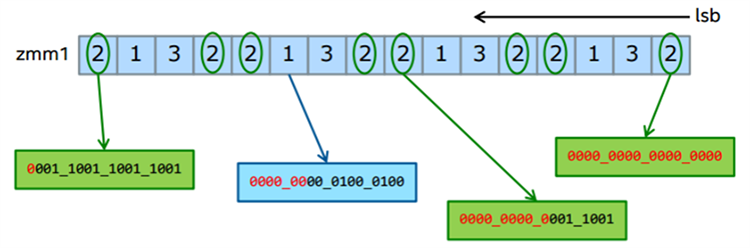
Figure 9. Diagram of mask generation for VPCONFLICT.
In order to benefit from CDI, use Intel compilers version 16.0 in Intel® C++ Composer XE 2016, which will recognize potential run-time conflicts and generate VPCONFLICT loops automatically.
Transcendental support
Additional 512-bit instruction extensions have been provided to accelerate certain transcendental mathematic computations and can be found in the instructions VEXP2PD, VEXP2PS, VRCP28xx, and VRSQRT28xx, also known as Intel AVX-512 exponential and reciprocal instructions. These can benefit some finance applications.
Compiler support
Intel AVX-512 optimizations are included in Intel compilers version 16.0 in Intel C++ Composer XE 2016 and the GNU Compiler Collection (GCC) 5.0 (NASM 2.11.08 and binutils 2.25). Table 8 summarizes compiler arguments for optimization on the Intel Xeon processor D-2100 product family microarchitecture with Intel AVX-512.
Table 9. Summary of Intel® Xeon® processor D-2100 product family compiler optimizations.
| Compiler Optimizations for Intel® AVX-512 on Intel® Xeon® processor D-2100 product family microarchitecture |
|
|---|---|
| Intel® Compilers version 16.0 or greater |
GCC 5.0 or greater |
| General optimizations |
|
| -QxCOMMON-AVX512 on Windows* with Intel Compilers |
-mavx512f -mavx512cd on Linux with Intel Compilers |
| Intel Xeon processor D-2100 product family specific optimizations |
|
| -QxCORE-AVX512 on Windows with Intel Compilers |
-mavx512bw -mavx512dq -mavx512vl -mavx512ifma -mavx512vbmi on Linux with Intel Compilers |
For more information see the Intel® Architecture Instruction Set Extensions Programming Reference.
Intel® speed shift technology
The Intel Xeon processor D-1500 product family introduced hardware power management (HWPM), a new optional processor power management feature in the hardware that liberates the operating system from making decisions about processor frequency. HWPM allows the platform to provide information on all available constraints, allowing the hardware to choose the optimal operating point. Operating independently, the hardware uses information that is not available to software and is able to make a more optimized decision in regard to the p-states and c-states. The Intel Xeon processor D-2100 product family expands on this feature by providing a broader range of states that it can affect as well as a finer level of granularity and microarchitecture observability via the package control unit (PCU). On the Intel Xeon processor D-1500 product family the HWPM was autonomous, also known as out-of-band mode, and oblivious to the operating system. The Intel Xeon processor D-2100 product family allows for this as well, but also offers the option for a collaboration between the HWPM and the operating system, known as native mode. The operating system can directly control the tuning of the performance and power profile when and where it is desired, while elsewhere the PCU can take autonomous control in the absence of constraints placed by the operating system. In native mode, the Intel Xeon processor D-2100 product family is able to optimize frequency control for legacy operating systems, while providing new usage models for modern operating systems. The end user can set these options within the BIOS; see your OEM BIOS guide for more information. Modern operating systems that provide full integration with native mode include Linux*, starting with kernel 4.10, and Windows Server* 2016.
Intel® QuickAssist Technology (Intel® QAT)
Intel® QAT accelerates and compresses cryptographic workloads by offloading the data to hardware capable of optimizing those functions. This makes it easier for developers to integrate built-in cryptographic accelerators into network, storage, and security applications. In the case of the Intel Xeon processor D-2100 product family, the third-generation Intel QAT is integrated into the hardware, and offers outstanding capabilities including up to 100Gbs crypto, 100Gbs compression, and 100K ops RSA2K.
Segments that can benefit from the technology include the following:
- Server: secure browsing, email, search, big-data analytics (Hadoop*), secure multitenancy, IPsec, SSL/TLS, OpenSSL
- Networking: firewall, IDS/IPS, VPN, secure routing, web proxy, WAN optimization (IP comp), 3G/4G authentication
- Storage: real-time data compression, static data compression, secure storage
Supported algorithms include the following:
- Cipher algorithms: (A)RC, AES, 3DES, Kasumi, Snow3G, and ZUC
- Hash/authentication algorithms supported: MD5, SHA1, SHA-2, SHA-3, HMAC, AES-XCBC-MAC, Kasumi, Snow 3G, and ZUC
- Public key cryptography algorithms: RSA, DSA, Diffie-Hellman (DH), ECDSA, ECDH
ZUC and SHA-3 are new algorithms that are included in the third generation of Intel QAT.
Intel® Key Protection Technology (Intel® KPT) is a new supplemental feature of Intel QAT that can be found on the Intel Xeon processor D-2100 product family. Intel KPT was developed to help secure cryptographic keys from platform-level software and hardware attacks when the key is stored and used on the platform. This new feature focuses on protecting keys during runtime usage and is embodied within tools and techniques, and supports both OpenSSL and PKCS#11 cryptographic frameworks.
For a more detailed overview see Intel QuickAssist Technology for Storage, Server, Networking and Cloud-Based Deployments. Programming and optimization guides can be found on the 01 Intel Open Source website.
Internet wide area RDMA protocol (iWARP)
IWARP is a technology that allows network traffic managed by the network interface controller (NIC) to bypass the kernel, which thus reduces the impact on the processor due to the absence of network-related interrupts. This is accomplished by the NICs communicating with each other via queue pairs to deliver traffic directly into the application user space. Large storage blocks and virtual machine migration tend to place more burden on the CPU due to the network traffic. This is where iWARP can be of benefit. Through the use of the queue pairs it is already known where the data needs to go and thus it is able to be placed directly into the application user space. This eliminates extra data copies between the kernel space and the user space that would normally occur without iWARP.
For more information see the information video on Accelerating Ethernet with iWARP Technology.
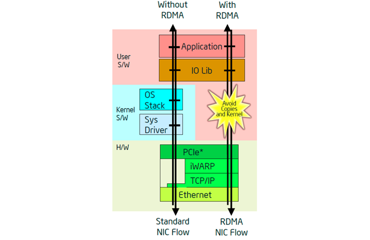
Figure 10. iWARP comparison block diagram.
Select models of the Intel Xeon processor D-2100 product family have integrated Intel® Ethernet connections with up to 4x10 GbE/1 Gb connections that include support for iWARP. This new feature can benefit various segments including network function virtualization and software-defined infrastructure. It can also be combined with the Data Plane Development Kit to provide additional benefits with packet forwarding.
iWARP uses Verb APIs to talk to each other instead of traditional sockets. For Linux, OFA Open Fabrics Enterprise Distribution (OFED) provides Verb APIs, while Windows* uses Network Direct APIs. Contact your Linux distribution to see if it supports OFED verbs, and on Windows, support is provided starting with Windows Server 2012 R2 or newer.
RAS features
The Intel Xeon processor D-2100 product family includes new RAS (reliability, availability, and serviceability) features. Listed below is a comparison of the RAS features from the previous generation.
Table 10. RAS feature summary table.
| Feature |
Intel® Xeon® Processor D-1500 Product Family |
Intel® Xeon® Processor D-2100 Product Family |
|---|---|---|
| MCA and Corrected Machine Check Interrupt (CMCI) |
Yes |
Yes |
| MCA Bank Error Control (Cloaking) |
Yes |
Yes |
| PCI Express Hot-Plug |
Yes1 |
Yes |
| PCI Advanced Error Reporting |
Yes |
Yes |
| PCI Express "Stop and Scream" |
Yes1 |
Yes |
| PCI Express ECRC (End-to-End CRC) |
Yes1 |
Yes |
| Corrupt Data Containment Mode - Uncore (Poisoning supported in uncore only / no recovery) |
Yes |
Yes |
| Corrupt Data Containment Mode - Core |
No |
No |
| x4 Single Device Data Correction (SDDC) |
Yes |
Yes |
| Memory Mirroring |
No |
Yes |
| Memory Demand/Patrol Scrubbing |
Yes |
Yes |
| Data Scrambling with Command and Address |
Yes |
Yes |
| Memory Rank Sparing |
No |
Yes |
| Enhanced SMM |
Yes |
Yes |
1. Only available on PCIe Gen3 ports.
Intel® Volume Management Device (Intel® VMD)
Intel® VMD is a hardware technology on the Intel Xeon processor D-2100 product family primarily to improve the management of high-speed solid state drives (SSDs). Previously, SSDs were attached to a Serial ATA (SATA) or other interface type and managing them through software was acceptable. When we move toward directly attaching the SSDs to a PCIe* interface in order to improve bandwidth, software management of those SSDs adds more delays. Intel VMD uses hardware to mitigate these management issues rather than completely relying on software. This is accomplished by the Intel provided NVMe* driver, which works in conjunction with Intel VMD. The NVMe driver allows restrictions that might have been placed on it by an operating system to be bypassed. This means that features like hot insert could be available for an SSD even if the operating system doesn't provide it, and the driver can also provide support for third-party vendor NVMe non-Intel solid state drives.
Intel® Boot Guard
Intel® Boot Guard adds another level of protection by performing a cryptographic Root of Trust for Measurement of the early firmware platform storage device, such as the trusted platform module or Intel® Platform Trust Technology. It can also cryptographically verify early firmware using OEM-provided policies. Unlike Intel® Trusted Execution Technology (Intel® TXT), Intel Boot Guard doesn't have any software requirements; it is enabled at the factory and it cannot be disabled. Intel Boot Guard operates independently of Intel TXT but it is also compatible with it. Intel Boot Guard reduces the chance of malware exploiting the hardware or software components.
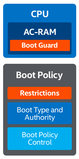
Figure 11. Intel Boot Guard secure boot options.
Three Secured Boot Options On Purley:
- Measured Boot
Boot Guard puts cryptographic measurement of the Early Firmware* into the platform protected storage device such as TPM or the Platform Trust Technology (PTT) - Verified Boot
Boot Guard cryptographically verifies the Early Firmware using the OEM provided policies. - Measured + Verified Boot
Performs both of the above actions.
Early Firmware
Setup Memory
Loads next block into memory
Continues with verification and/or measurements
Platform Firmware
Continue Verification or Measurement
UEFI 2.3.1 Secure boot for verification
TPM 1.2/2.0/PTT for measurement
Platform storage extensions
Platform storage extensions provides smarter and more cost-effective storage solutions through integrated technologies that accelerate data movement, protect data, and simplify data management. This is accomplished through different features such as Intel® QuickData Technology, which provides a direct memory access (DMA) engine within the SoC, enabling data copies by dedicated hardware instead of the CPU. Asynchronous DRAM refresh (ADR) helps preserve key data in battery-backed memory in the event of a loss in power. Non-transparent bridging enables redundancy via PCI Express. Lastly, end-to-end CRC protection is provided for the PCIe I/O subsystem.
The Innovation Engine
The Innovation Engine (IE) is an embedded core within the SoC. It is similar to Intel® Management Engine (Intel® ME), with some privilege and I/O differences. The IE is designed to assist OEMs in providing a more secure form of the Intel ME. IE code is cryptographically bound to the OEM, and code that is not authenticated by the OEM will not load. The system can operate normally without having to activate IE because it is an optional feature.
For cloud and embedded segments, the basic manageability without cost, space, or power of a Baseboard Management Controller (BMC) can be attractive. The IE runs simple management applications (for example, Intelligent Platform Management Interface (IPMI)) and network stack for out of band operations.
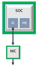
Figure 12. BMC-less manageability for lightweight requirements.
For the enterprise segment, IE can be of value for improving system performance by reducing BMC round trips or System Management Mode (SMM) interrupts on the CPU. IE runs OEM-specific BMC- or BIOS-assist software.
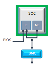
Figure 13. BMC- or BIOS-assisted configuration.
For more in-depth enterprise-level needs, IE and ME can work together to provide new or enhanced usage models using telemetry and controls provided by Intel. The IE can communicate with the ME to pull in telemetry data and provide additional processing capability.
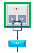
Figure 14. IE provides enhancement to Intel® ME firmware.
Intel® Node Manager (Intel® NM)
Intel® NM is a core set of power management features that provide a smart way to optimize and manage power, cooling, and compute resources in the data center. This server management technology extends component instrumentation to the platform level and can be used to make the most of every watt consumed in the data center. First, Intel NM reports vital platform information such as power, temperature, and resource utilization using standards-based, out-of-band communications. Second, it provides fine-grained controls such as helping with reduction of overall power consumption or maximizing rack loading, to limit platform power in compliance with IT policies. This feature can be found across Intel's product segments, including the Intel Xeon SoC D-2100 product family, providing consistency within the data center.
The Intel Xeon SoC D-2100 product family includes the fourth generation of Intel NM, which extends control and reporting to a finer level of granularity than on the previous generation. To use this feature you must enable the BMC LAN and the associated BMC user configuration at the BIOS level, which should be available under the server management menu. The Intel NM Programmer's Reference Kit is simple to use and requires no additional external libraries to compile or run. All that is needed is a C/C++ compiler and to then run the configuration and compilation scripts.
Table 11. Intel® NM fourth-generation features.
| Capabilities | Intel® Node Manager 4.0 | |
|---|---|---|
| Telemetry & monitoring | Monitor platform power consumption | |
| Monitor inlet airflow temperature | ||
| Support shared power supplies | ||
| Monitor CPU package and memory power consumption | ||
| PMBus support | ||
| BMC power reading support | ||
| Support Voltage Regulator & Current Monitor configuration | ||
| Hot-swap controller support | ||
| Power Component Telemetry | ||
| Power management during operation | Set platform power limits & policies ( 16 policies ) | |
| API support | ACPI power meter support | |
| DCMI API support | ||
| Node Manager IPMI API support over SMBus | ||
| ACPI support | ||
| Node Manager IPMI API support over IE Sideband Interface | ||
| Power management during boot | Set power optimized boot mode in BIOS (during next reboot) | |
| Configure core(s) to be disabled by BIOS (during next reboot) | ||
| Set platform power limit during boot | ||
| Performance & Characterization | CPU, Memory, I/O utilization metrics | |
| Compute utilization per Second (CUPS) | ||
| Hardware Protection | SMART/CLST | |
| PSU events | Reduce platform power consumption during power supply event (PSU failover/undercurrent) | |
| Assess platform parameters | Node Manager Power Thermal Utility (determines max, min & efficient power levels) | |
| Platform temp excursions | Reduce platform power consumption during inlet airflow excursion |
Author
David Mulnix is a software engineer and has been with Intel Corporation for over 20 years. His areas of focus includes software automation, server power, and performance analysis, and he has contributed to the development support of the Server Efficiency Rating Tool*.
Contributors
Akhilesh Kumar and Elmoustapha Ould-ahmed-vall.
Resources
Intel® 64 and IA-32 Architectures Software Developer's Manual (SDM)
Intel® Architecture Instruction Set Extensions Programming Reference
Intel® Memory Protection Extensions Enabling Guide
Intel Node Manager Programmer's Reference Kit
Open Source Reference Kit for Intel® Node Manager
How to set up Intel® Node Manager
Intel® Performance Counter Monitor (Intel® PCM), - A better way to measure CPU utilization